SENSORS AND ELECTRONICS
One advantage of the electron beam welding process for electronic packaging is the relatively low heat input compared to other welding processes such as tungsten inert gas (TIG). The shape of the fusion zone can be altered and optimised using high-speed deflection of the electron beam, which may be relatively small for sealing purposes and deeper if required for more structural applications.
The process is done in a vacuum which prevents oxidation, and the low heat input minimises the risk of damage to sensitive electronics.
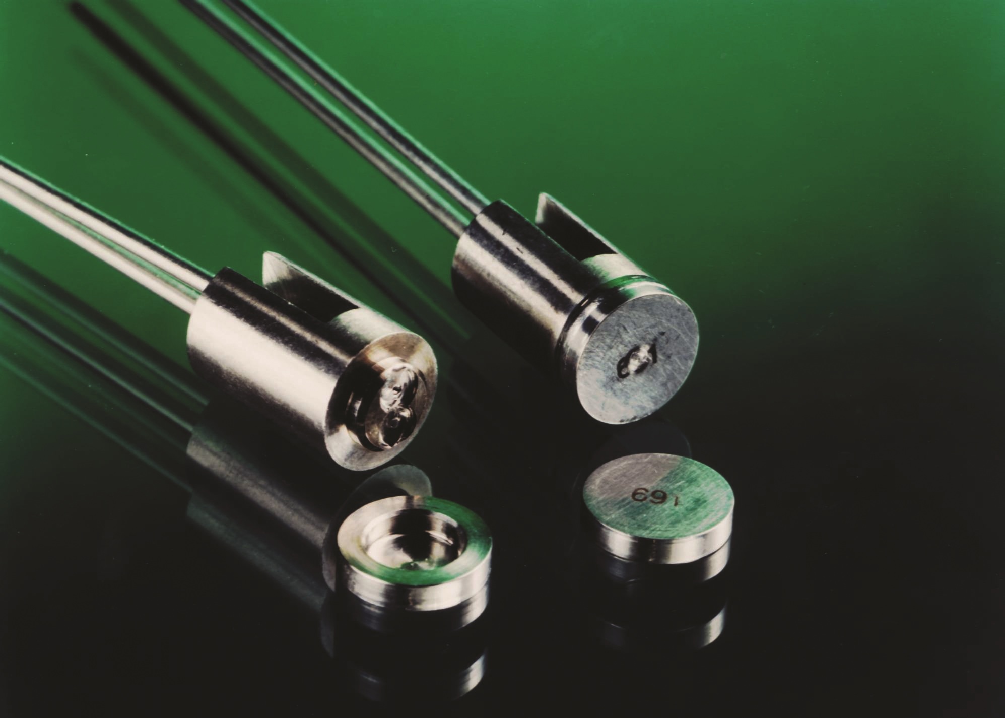
Semiconductors
Electron beam welding is used to join many components in the semiconductor industry where high-quality, defect-free welds are required.
Low porosity in welds is essential for ensuring high levels of cleanliness are maintained in service and the low overall heat input of electron beam welding also results in minimal distortion which reduces the amount of post-weld machining.